Photonic Integrated Circuits Accelerating Miniaturization

Driving a Technological Shift: The Power of Photonic Integrated Circuits
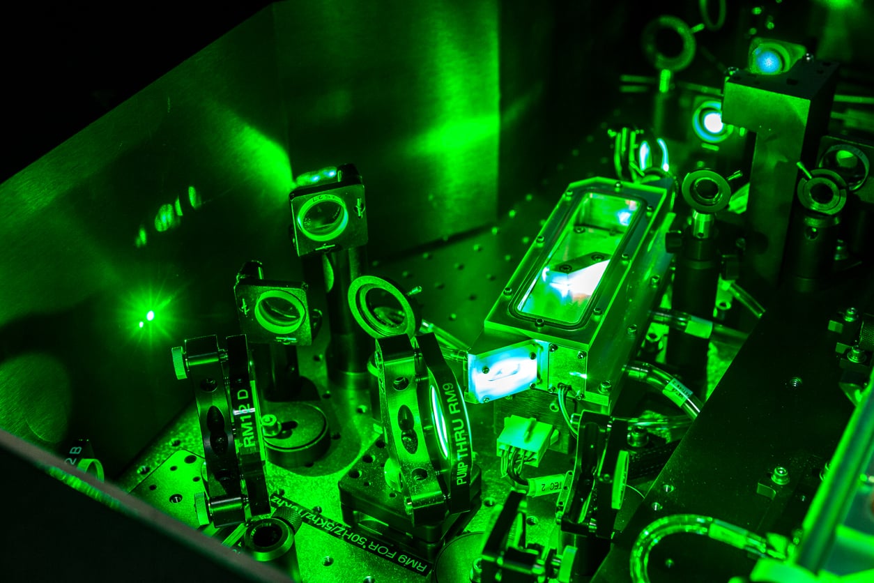
Photonic integrated circuits (PICs) are rapidly redefining modern technology. By consolidating complex optical components onto a single chip, PICs are spurring advances in applications as wide-ranging as LiDAR, optical communications, and chip-to-chip interconnects. The ability to miniaturize essential photonic elements has forged new possibilities in industries that demand smaller form factors, reduced power consumption, and unprecedented data throughput.
Over the last 57 years, Rudzinsky Associates has supported progress in lasers, optics, imaging, optoelectronics, and photonics by connecting pioneering companies with key professionals. This synergy of talent and technology has helped accelerate breakthroughs in wafer-level manufacturing and 3D integration. As investment capital pours into both startups and established tech giants, the photonics sector is positioned to keep expanding, transforming data transmission, sensing, and computing technologies in the process.
Seamless Integration with Photonic Circuits: From Discrete Optics to Monolithic Systems
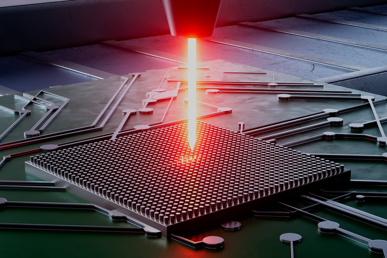
Historically, optical systems relied on arrays of separate components—mirrors, lenses, amplifiers—each requiring precise mechanical placement. With the advent of photonic circuits, these bulky assemblies are being replaced by monolithic implementations. Silicon photonics, for example, makes use of well-established semiconductor fabrication processes to produce modulators, waveguides, and detectors on the same piece of silicon.
By merging multiple functions into a single chip, manufacturers dramatically reduce alignment complexity, packaging overhead, and energy consumption. The result is a leap forward in size, power efficiency, and overall performance. Whether multiplexing signals in data centers or directing laser beams for precision measurements, monolithic photonic integration offers higher reliability and simpler designs that lower the barriers to practical deployment.
Leveraging Established Semiconductor Infrastructure for Photonics
The widespread adoption of PICs is closely tied to the ability to use existing semiconductor manufacturing infrastructure. Because photonic chip production parallels the processes behind electronic integrated circuits, companies can quickly iterate designs, scale up production, and lower costs. Many organizations partner with outsourced semiconductor foundries to fabricate chips while focusing in-house engineering on system integration, custom applications, and proprietary design enhancements.
This alignment with established supply chains fosters faster prototyping and higher yields. As a result, photonic technologies can move from research labs to high-volume manufacturing with fewer hurdles, reinforcing their growing influence in markets that demand both high performance and cost-effectiveness.
Transforming Optical Communications and Modern Data Centers with PICs
One of the most visible beneficiaries of integrated photonics is the optical communications sector. Worldwide data traffic continues to surge, causing data centers to grapple with rising energy bills and bandwidth limitations. PICs offer a more efficient hardware-level approach, enabling transceivers, modulators, and multiplexing units to coexist on a single chip. By consolidating these functions, PIC-based solutions boost signal integrity while cutting power consumption—a cornerstone for next-generation data center infrastructure.
Although traditional electronic interconnects still handle substantial information flow, they encounter practical limits in speed and thermal dissipation as data rates escalate toward the terabit threshold. Photons traveling through optical waveguides circumvent many of these constraints. Key benefits include:
- Higher Bandwidth: Multiple optical channels can transmit large quantities of data simultaneously, free from electromagnetic interference.
- Reducing Power Demands: Moving signal processing from electronic to photonic domains diminishes heat generation and cooling needs.
- Smaller Footprint: Integrated waveguides and optical switches occupy far less real estate than comparable electronic components, facilitating further miniaturization.
With telecom providers and hyperscale data centers striving to enhance energy efficiency, PIC-driven solutions increasingly replace or supplement legacy electrical systems. This evolution supports ever-higher capacities, from cloud computing platforms to bandwidth-hungry services like virtual reality and high-resolution video streaming.
Evolving Network Architecture: Photonic Innovations and ROADMs
Beyond transceivers and short-reach interconnects, photonic integration also reshapes broader network architecture. Multi-wavelength photonic interfaces allow data center operators to push more data traffic through each fiber strand, extending the usefulness of existing infrastructures. Meanwhile, integrated reconfigurable optical add-drop multiplexers (ROADMs) enable dynamic bandwidth management, tailoring resources to fluctuating network demands.
By combining high throughput with reconfigurable capabilities, integrated photonics helps data centers become more scalable, adaptable, and cost-efficient. Network operators can route and allocate data in near-real time to handle evolving workflows—an approach that sets the scene for future advancements in edge computing and distributed architectures.
Advanced Materials and Cutting-Edge Fabrication for PICs
PIC performance hinges on ongoing research into semiconductor materials. While silicon photonics remains dominant for wavelengths near 1310 nm and 1550 nm—ubiquitous in telecommunications—indium phosphide (InP) substrates and other compound semiconductors excel when alternate emission or detection ranges are necessary. Hybrid solutions integrate multiple materials on a single die, ensuring that specific device functionalities can be fine-tuned without sacrificing efficiency or compatibility.
Some key fabrication approaches fostering commercial viability include:
- Wafer-Level Packaging (WLP): Streamlines mass production by handling encapsulation and alignment at the wafer scale, minimizing the complexity and cost of individual device assembly.
- 3D Integration: Stacks optical and electronic components vertically, raising the potential for packing greater functionality into a small footprint with shorter interconnect distances.
- Advanced Lithography: Deploying deep ultraviolet (DUV) and extreme ultraviolet (EUV) technologies extends the precision and density of waveguide patterning, unlocking higher performance and tighter feature sizes.
These manufacturing innovations reflect a push to commercialize advanced photonic systems at scale. By accepting a broader set of materials, fabricating smaller and more precise features, and refining packaging capabilities, PIC technology becomes accessible to industries from aerospace to biomedical imaging.
Overcoming Thermal Management and Yield Challenges
Despite the significant evolution of PIC manufacturing, hurdles remain—most notably surrounding thermal management and device yield. High optical power densities can spark hot spots that impair performance or shorten component lifetimes. Re-engineered waveguide geometries, integrated heat spreaders, improved airflow, and even microfluidic cooling are under development to mitigate these thermal impacts.
On the yield side, stabilizing processes to achieve uniform device performance at scale is essential to lowering costs. Rigorous testing protocols and real-time process monitoring aim to detect subtle defects early. By fine-tuning each stage—material deposition, lithography, and packaging—manufacturers can approach electronic-integrated-circuit-like yields, significantly improving cost-effectiveness for end users.
Branching into New Applications: LIDAR, Healthcare, and Beyond
Although data transmission remains central to PIC adoption, photonic integration is making inroads in fields like LiDAR, healthcare, and remote sensing. Mechanical scanning LiDAR, with its spinning assemblies, is gradually giving way to solid-state integrative solutions. These on-chip LiDAR designs offer longer range, higher resolution, and fewer mechanical points of failure. The result: more compact form factors suited to autonomous vehicles, robotic platforms, and mapping drones.
In medical diagnostics, PICs are facilitating the rise of miniaturized, high-resolution imaging devices. Integrated optical coherence tomography (OCT) platforms yield detailed images of soft tissues with minimal intrusion. Meanwhile, lab-on-a-chip photonic sensors directly detect biomarkers or pathogens, compressing entire diagnostic workflows into portable or even wearable devices. These innovations mark a significant leap forward in patient care, enabling precision medicine that rests on fast, accurate, and less cumbersome diagnostic tools.
Empowering Quantum Computing and Secure Communications
Quantum computing represents another frontier catalyzed by photonic integration. Photons used as quantum bits (qubits) can operate at room temperature and are relatively resistant to decoherence compared to some superconducting approaches. Recent advances show promise for on-chip quantum photonics, incorporating beam splitters, interferometers, and single-photon detectors to create sophisticated quantum circuits.
Alongside quantum computing, secure communications benefit from quantum key distribution (QKD), which exploits the fundamental laws of physics to detect any eavesdropping attempts. PICs are helping to miniaturize these QKD systems, potentially paving the way for widespread adoption of ultra-secure data channels across finance, defense, and other sensitive sectors.
Building a Skilled Workforce to Advance Photonic Technology
As PICs gain momentum in diverse applications, demand grows for experts in optical design, materials science, packaging, and systems integration. Designing photonic circuits requires a hybrid understanding of how light and electronics coexist on ever-shrinking chips. Professionals in this space must also grasp the nuances of high-volume manufacturing, testing, and reliability—skills that enable companies to move from the lab to the marketplace.
Effective team composition often pairs photonics specialists with software developers, mechanical engineers, and electronics experts. This cross-functional approach speeds product cycles and leads to platforms that fully harness photonics’ potential. By bridging these disciplines, engineers can optimize components for performance, address key manufacturing constraints, and achieve faster time-to-market for next-generation solutions.
Sustaining Growth in an Era of Integrated Photonics
Organizations that spearhead the PIC revolution juggle a need for rapid innovation with the practical considerations of market viability. The specialized nature of photonic research and development underscores the importance of seasoned leadership and collaborative engineering teams. Ongoing success relies on attracting talent adept at materials engineering, optical simulation, device packaging, and large-scale system integration.
Through strategic recruitment, companies can balance the technical complexity of PICs with commercial imperatives. This synergy fosters efficient prototyping, stable supply chains, and ultimately superior products—whether for high-throughput data centers, state-of-the-art medical diagnostics, or advanced sensor networks.
Anticipating the Next Wave of Photonic Innovation: Emerging Opportunities
The trajectory of photonic integration appears boundless. As data centers continue to call for ultrafast interconnects, autonomous vehicles demand high-performance LiDAR, and medicine evolves toward miniaturized diagnostic systems, PICs are poised to become standard components across countless domains. Even personal devices may harness integrated photonics to deliver functionalities barely conceivable a decade ago.
Future breakthroughs will likely revolve around more sophisticated materials, tighter couplings to electronics, and increasingly seamless design workflows. As manufacturing techniques mature, engineers will harness improved yields, advanced assembly methods, and competitive pricing structures. This convergence will make cutting-edge PIC technology feasible in large-scale deployments, from 5G communication networks to individualized healthcare tools.
By continuously refining thermal solutions and boosting production yields, the photonics industry edges closer to delivering on the promise of compact, power-efficient, and intelligent hardware that offers game-changing performance. As labs and industrial conglomerates alike race to define the next milestones, the realm of integrated photonics grows richer and more accessible.
To remain at the forefront of these transformative changes, securing the right expertise is critical. Rudzinsky Associates, with decades of experience in optics and photonics, stands ready to help organizations identify and recruit the specialized talent that drives effective PIC development. Through a deep understanding of industry needs, we ensure that companies can assemble the teams necessary to excel in today’s rapidly evolving photonics landscape—empowering them to chart new frontiers where on-chip optical technologies continuously redefine the possible.